
Summary
- Infineon plans approximately €1.1bn of investment at its Villach semiconductor site through 2034.
- Initial production on 300mm GaN wafers is planned for late 2027, subject to manufacturing ramp-up.
- European Commission approval covers €319m in state aid, with a formal Austrian funding commitment still expected.
Infineon Technologies plans to invest approximately €1.1bn in high-volume gallium nitride power semiconductor manufacturing at its Villach site in Austria by 2034. The project will use 300mm wafers and existing cleanroom infrastructure, with the start of production scheduled for the end of 2027.
AI power supplies are among the markets Infineon intends the new manufacturing capacity to serve, together with electricity infrastructure, electric vehicles, robotics and consumer electronics. The 27 October plan is an industrial supply-chain investment, not a data-centre capacity announcement, and the company has not allocated a disclosed share of the proposed output to data-centre customers.
The project is expected to receive support under the European Chips Act. The European Commission has approved €319m in state aid, while Infineon says the formal funding commitment from Austria’s relevant ministry is still expected. Commission approval of aid is not the same as confirmation that every euro has been disbursed.
Why wafer diameter affects production
Power semiconductors provide the switching and conversion functions required as electricity passes between grid connections, uninterruptible power supplies, power distribution equipment and server hardware. Different materials and designs suit different conversion voltages, thermal requirements and switching regimes.
Gallium nitride has properties that can support high-frequency switching and lower losses in suitable applications. In power supplies, those characteristics can reduce the size of passive components and limit the heat created by conversion, provided the surrounding circuit, thermal design and control strategy are appropriately engineered.
GaN also faces competition from silicon and silicon carbide devices, which serve overlapping but different voltage, efficiency, reliability and cost requirements. Component choice depends on the complete converter design, switching frequency, manufacturing maturity and qualification requirements. The material alone does not establish system efficiency.
Infineon says a 300mm wafer can produce approximately 2.3 times as many chips as a 200mm wafer of comparable process design. The physical area ratio is an important part of that improvement, but higher gross die counts do not by themselves determine manufacturing yield, finished product cost or the number of qualified devices shipped.
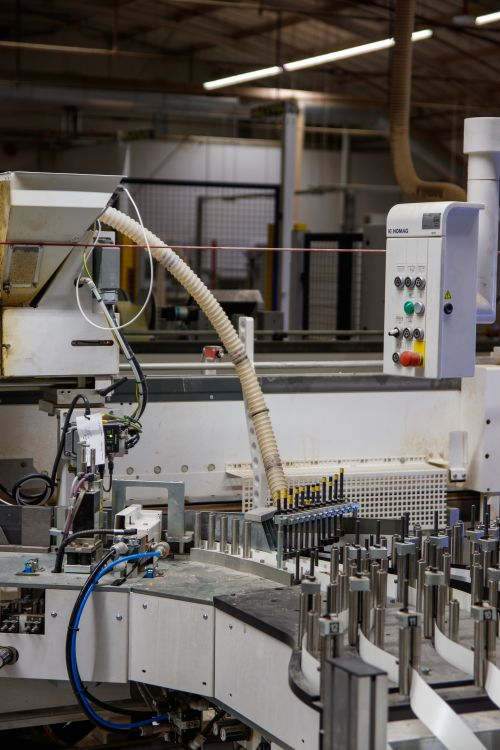
Moving a material system to high-volume 300mm production is therefore a manufacturing programme as well as an electrical design development. Processes must maintain consistent film quality, defect control, device characteristics and testing across the larger surface. Infineon says it previously demonstrated processing of 300mm GaN wafers and is now transferring that technology towards industrial-scale output.
Data-centre power demand
Large AI racks concentrate substantial computing loads into relatively small spaces. Delivering electricity efficiently to those loads requires several conversion steps, often moving from site-level alternating current through higher-voltage distribution and finally to the low-voltage rails required by chips and other hardware.
Each conversion stage incurs losses that become heat. Improving an individual stage can reduce waste, but a device’s peak efficiency is not equivalent to the efficiency of a complete site-wide electrical chain. Practical performance also depends on operating load, thermal conditions, protection design and the number of stages used.
Manufacturing expansion could increase the availability of components needed by suppliers developing higher-density power conversion. It would be inaccurate, however, to turn Infineon’s intended output into a forecast of installed AI rack power or to assume that a named operator has placed orders for parts that are not identified in the announcement.
Infineon’s separate high-voltage power distribution reference design announced on the same day illustrates a possible application of advanced conversion technologies. That board is a product evaluation platform and is a distinct story from the investment in Villach manufacturing capacity. The former concerns electrical architecture; the latter concerns the industrial supply chain capable of producing devices.
At Villach, Infineon intends to use and upgrade existing cleanroom facilities rather than start with an entirely separate greenfield manufacturing location. This approach may help bring new processing capacity into use, but the company has not published a full annual wafer-output schedule or a detailed breakdown of construction, equipment and process investment.
Production is expected to start at the end of 2027, with the subsequent ramp aligned to demand. Such a timetable should not be presented as immediate mass availability across every GaN product family. Qualification, product integration and customer adoption can take place at different rates after initial manufacturing begins.
Austria already hosts a substantial power-electronics research and manufacturing ecosystem around Villach. Infineon expects the project to reinforce that base, including collaboration with research organisations and other technology companies. The wider industrial benefit is an announced intention; the future distribution of jobs, output and downstream investment remains to be demonstrated.
Production of 300mm gallium nitride devices is scheduled to begin at Villach by the end of 2027, followed by an investment and ramp-up programme extending towards 2034. Data-centre electrical equipment suppliers could benefit from greater component availability, but no new operating data-centre megawatts or named customer orders were disclosed with the investment.

